- Links:
开板板简介
管脚定义
- 下面数据来源于
DE0_Nano_User_Manual.pdf的Chapter 3-3.5 Expansion headers.
GPIO-0 Pin Assignments
| Signal Name | FPGA Pin No. | Descritption | I/O Standard |
|---|---|---|---|
| GPIO_0_IN0 | PIN_A8 | GPIO Connection DATA | 3.3V |
| GPIO_00 | PIN_D3 | GPIO Connection DATA | 3.3V |
| GPIO_0_IN1 | PIN_B8 | GPIO Connection DATA | 3.3V |
| GPIO_01 | PIN_C3 | GPIO Connection DATA | 3.3V |
| GPIO_02 | PIN_A2 | GPIO Connection DATA | 3.3V |
| GPIO_03 | PIN_A3 | GPIO Connection DATA | 3.3V |
| GPIO_04 | PIN_B3 | GPIO Connection DATA | 3.3V |
| GPIO_05 | PIN_B4 | GPIO Connection DATA | 3.3V |
| GPIO_06 | PIN_A4 | GPIO Connection DATA | 3.3V |
| GPIO_07 | PIN_B5 | GPIO Connection DATA | 3.3V |
| GPIO_08 | PIN_A5 | GPIO Connection DATA | 3.3V |
| GPIO_09 | PIN_D5 | GPIO Connection DATA | 3.3V |
| GPIO_010 | PIN_B6 | GPIO Connection DATA | 3.3V |
| GPIO_011 | PIN_A6 | GPIO Connection DATA | 3.3V |
| GPIO_012 | PIN_B7 | GPIO Connection DATA | 3.3V |
| GPIO_013 | PIN_D6 | GPIO Connection DATA | 3.3V |
| GPIO_014 | PIN_A7 | GPIO Connection DATA | 3.3V |
| GPIO_015 | PIN_C6 | GPIO Connection DATA | 3.3V |
| GPIO_016 | PIN_C8 | GPIO Connection DATA | 3.3V |
| GPIO_017 | PIN_E6 | GPIO Connection DATA | 3.3V |
| GPIO_018 | PIN_E7 | GPIO Connection DATA | 3.3V |
| GPIO_019 | PIN_D8 | GPIO Connection DATA | 3.3V |
| GPIO_020 | PIN_E8 | GPIO Connection DATA | 3.3V |
| GPIO_021 | PIN_F8 | GPIO Connection DATA | 3.3V |
| GPIO_022 | PIN_F9 | GPIO Connection DATA | 3.3V |
| GPIO_023 | PIN_E9 | GPIO Connection DATA | 3.3V |
| GPIO_024 | PIN_C9 | GPIO Connection DATA | 3.3V |
| GPIO_025 | PIN_D9 | GPIO Connection DATA | 3.3V |
| GPIO_026 | PIN_E11 | GPIO Connection DATA | 3.3V |
| GPIO_027 | PIN_E10 | GPIO Connection DATA | 3.3V |
| GPIO_028 | PIN_C11 | GPIO Connection DATA | 3.3V |
| GPIO_029 | PIN_B11 | GPIO Connection DATA | 3.3V |
| GPIO_030 | PIN_A12 | GPIO Connection DATA | 3.3V |
| GPIO_031 | PIN_D11 | GPIO Connection DATA | 3.3V |
| GPIO_032 | PIN_D12 | GPIO Connection DATA | 3.3V |
| GPIO_033 | PIN_B12 | GPIO Connection DATA | 3.3V |
GPIO-1 Pin Assignments
| Signal Name | FPGA Pin No. | Descritption | I/O Standard |
|---|---|---|---|
| GPIO_1_IN0 | PIN_T9 | GPIO Connection DATA | 3.3V |
| GPIO_10 | PIN_F13 | GPIO Connection DATA | 3.3V |
| GPIO_1_IN1 | PIN_R9 | GPIO Connection DATA | 3.3V |
| GPIO_11 | PIN_T15 | GPIO Connection DATA | 3.3V |
| GPIO_12 | PIN_T14 | GPIO Connection DATA | 3.3V |
| GPIO_13 | PIN_T13 | GPIO Connection DATA | 3.3V |
| GPIO_14 | PIN_R13 | GPIO Connection DATA | 3.3V |
| GPIO_15 | PIN_T12 | GPIO Connection DATA | 3.3V |
| GPIO_16 | PIN_R12 | GPIO Connection DATA | 3.3V |
| GPIO_17 | PIN_T11 | GPIO Connection DATA | 3.3V |
| GPIO_18 | PIN_T10 | GPIO Connection DATA | 3.3V |
| GPIO_19 | PIN_R11 | GPIO Connection DATA | 3.3V |
| GPIO_110 | PIN_P11 | GPIO Connection DATA | 3.3V |
| GPIO_111 | PIN_R10 | GPIO Connection DATA | 3.3V |
| GPIO_112 | PIN_N12 | GPIO Connection DATA | 3.3V |
| GPIO_113 | PIN_P9 | GPIO Connection DATA | 3.3V |
| GPIO_114 | PIN_N9 | GPIO Connection DATA | 3.3V |
| GPIO_115 | PIN_N11 | GPIO Connection DATA | 3.3V |
| GPIO_116 | PIN_L16 | GPIO Connection DATA | 3.3V |
| GPIO_117 | PIN_K16 | GPIO Connection DATA | 3.3V |
| GPIO_118 | PIN_R16 | GPIO Connection DATA | 3.3V |
| GPIO_119 | PIN_L15 | GPIO Connection DATA | 3.3V |
| GPIO_120 | PIN_P15 | GPIO Connection DATA | 3.3V |
| GPIO_121 | PIN_P16 | GPIO Connection DATA | 3.3V |
| GPIO_122 | PIN_R14 | GPIO Connection DATA | 3.3V |
| GPIO_123 | PIN_N16 | GPIO Connection DATA | 3.3V |
| GPIO_124 | PIN_N15 | GPIO Connection DATA | 3.3V |
| GPIO_125 | PIN_P14 | GPIO Connection DATA | 3.3V |
| GPIO_126 | PIN_L14 | GPIO Connection DATA | 3.3V |
| GPIO_127 | PIN_N14 | GPIO Connection DATA | 3.3V |
| GPIO_128 | PIN_M10 | GPIO Connection DATA | 3.3V |
| GPIO_129 | PIN_L13 | GPIO Connection DATA | 3.3V |
| GPIO_130 | PIN_J16 | GPIO Connection DATA | 3.3V |
| GPIO_131 | PIN_K15 | GPIO Connection DATA | 3.3V |
| GPIO_132 | PIN_J13 | GPIO Connection DATA | 3.3V |
| GPIO_133 | PIN_J14 | GPIO Connection DATA | 3.3V |
Table 3-8 Pin Assignments for 2x13 Header
| Signal Name | FPGA Pin No. | Descritption | I/O Standard |
|---|---|---|---|
| GPIO_2[0] | PIN_A14 | GPIO Connection DATA[0] | 3.3V |
| GPIO_2[1] | PIN_B16 | GPIO Connection DATA[1] | 3.3V |
| GPIO_2[2] | PIN_C14 | GPIO Connection DATA[2] | 3.3V |
| GPIO_2[3] | PIN_C16 | GPIO Connection DATA[3] | 3.3V |
| GPIO_2[4] | PIN_C15 | GPIO Connection DATA[4] | 3.3V |
| GPIO_2[5] | PIN_D16 | GPIO Connection DATA[5] | 3.3V |
| GPIO_2[6] | PIN_D15 | GPIO Connection DATA[6] | 3.3V |
| GPIO_2[7] | PIN_D14 | GPIO Connection DATA[7] | 3.3V |
| GPIO_2[8] | PIN_F15 | GPIO Connection DATA[8] | 3.3V |
| GPIO_2[9] | PIN_F16 | GPIO Connection DATA[9] | 3.3V |
| GPIO_2[10] | PIN_F14 | GPIO Connection DATA[10] | 3.3V |
| GPIO_2[11] | PIN_G16 | GPIO Connection DATA[11] | 3.3V |
| GPIO_2[12] | PIN_G15 | GPIO Connection DATA[12] | 3.3V |
| GPIO_2_IN[0] | PIN_E15 | GPIO Input | 3.3V |
| GPIO_2_IN[1] | PIN_E16 | GPIO Input | 3.3V |
| GPIO_2_IN[2] | PIN_M16 | GPIO Input | 3.3V |
Table 3-9 Pin Assignments for ADC
| Signal Name | FPGA Pin No. | Descritption | I/O Standard |
|---|---|---|---|
| ADC_CS_N | PIN_A10 | Chip select | 3.3V |
| ADC_SADDR | PIN_B10 | Digital data input | 3.3V |
| ADC_SDAT | PIN_A9 | Digital data output | 3.3V |
| ADC_SCLK | PIN_B14 | Digital clock input | 3.3V |
JTAG

OpenRisc
GCC工具链
1 | ~$ git clone https://github.com/stffrdhrn/or1k-toolchain-build |
- 设置挂载目录变量,运行容器编译.如果
build-gcc.sh内的资源链接失效了,需要找一个替代修改它,如:QEMU_URL=https://github.com/vamanea/qemu-or32/archive/v2.0.2.tar.gz.
1 | # The location where you have tarballs, so they dont need to be |
- 编译成功后,如下:
1 | ls |
- 这里把
or1k-linux-9.0.1-20210204.tar.xz解压安装到本地,并设置相应的环境变量如下:1
2
3
4
5
6export ALTERA_PATH="/home/michael/3TB-DISK/intelFPGA_lite/20.1/"
export PATH=$PATH:$ALTERA_PATH/quartus/bin
export ARCH=openrisc
export CROSS_COMPILE=or1k-linux-
export PATH=$PATH:`pwd`/toolchain-rootfs/or1k-linux/bin - 或者单独编译
or1k-gcc1
2
3
4
5~$ git clone https://github.com/openrisc/or1k-gcc
~$ cd or1k-gcc/
~$ mkdir build-linux
~$ cd build-linux && ../configure && make -j4
~$ make install DESTPATH=<absolute path>
编译ORPSOC
1 | ~$ git clone https://github.com/mczerski/orpsoc-de0_nano |
编译Linux
1 | ~$ tar xvf linux-4.16.14.tar.xz |
烧写入bitstream
1 | ~$ cd orpsoc/boards/altera/de0_nano/syn/quartus/run |
连接串号
- 根据上面
GPIO的管脚定义,以及下面的信息,连接正确的rx,tx.
1 | cat boards/altera/de0_nano/syn/quartus/tcl/UART0_pin_assignments.tcl |
FuseSOC 试用
安装fuseSoc
1 |
|
安装fusesoc 库
- 从网络安装.
1 | ~$ fusesoc library add intgen https://github.com/openrisc/intgen.git |
- 从本地安装
1 | ~$ git clone https://github.com/openrisc/mor1kx-generic.git |
1 | ~$ fusesoc list-cores |
- 查看
fusesoc.conf配置.
1 | ~$ cat fusesoc.conf |
Fusesoc-demos
1 | fusesoc library add https://github.com/Oxore/fusesoc-demos |
RISC-V
- links:
安装Quartus20
- 这里只是安装QuartusLiteSetup-20.1.1.720-linux.run再加两个设备文件,没下载整个安装
tar包,总包体积在6.5GB左右.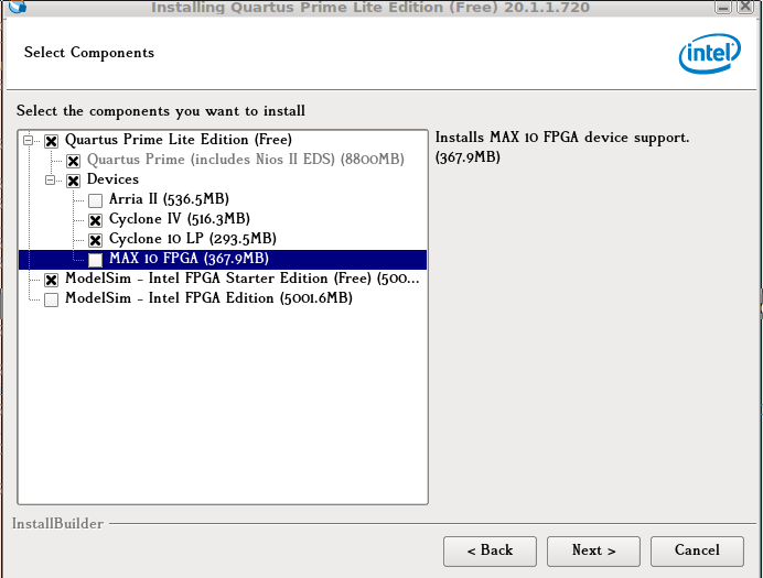
litex-boards测试编译
- 这里使用
litex-hub里的项目测试,Quartus安装到~/intelFPGA_lite/20.1/quartus目录下.注意,加上--load参数项,必须先运行jtagd服务,否则quartus_pgm无法进行jtag烧写.
1 | ~$ export PATH=~/riscv64-toolchain/bin:~/intelFPGA_lite/20.1/quartus/bin:$PATH |
- 其实最终的编译脚本是如下内容.
1 | linux-on-litex-vexriscv$ cat build/de0nano/gateware/build_de0nano.sh |
linux-on-litex-vexriscv编译测试
1 | ~$ cd linux-on-litex-vexriscv |
- 运行
--load参数时,需要确保jtagd是运行的,这里如下面所示,最终是使用quartus_pgm -m jtag -c USB-Blaster加载的.1
2
3
4
5
6
7
8
9
10
11
12
13
14
15
16[...]
Info: Command: quartus_pgm -m jtag -c USB-Blaster -o p;/home/michael/workspace-xilinx/RISC-V/litex-hub/litex/linux-on-litex-vexriscv/build/de0nano/gateware/de0nano.sof@1
Info (213046): Using programming cable "USB-Blaster on 127.0.0.1 [3-3]"
Info (213011): Using programming file /home/michael/workspace-xilinx/RISC-V/litex-hub/litex/linux-on-litex-vexriscv/build/de0nano/gateware/de0nano.sof with checksum 0x0085AEAF for device EP4CE22F17@1
Info (209060): Started Programmer operation at Sat Feb 26 11:35:48 2022
Info (209016): Configuring device index 1
Info (209017): Device 1 contains JTAG ID code 0x020F30DD
Info (209007): Configuration succeeded -- 1 device(s) configured
Info (209011): Successfully performed operation(s)
Info (209061): Ended Programmer operation at Sat Feb 26 11:35:49 2022
Info: Quartus Prime Programmer was successful. 0 errors, 0 warnings
Info: Peak virtual memory: 315 megabytes
Info: Processing ended: Sat Feb 26 11:35:49 2022
Info: Elapsed time: 00:00:32
Info: Total CPU time (on all processors): 00:00:00
通过JTAG-UART查看启动信息
- 这里脚本默认是选择
serial进行通信的,上面我在编译时选择了--uart-name=jtag_uart,想测试使用板的上USB JTAG的方式来进行uart通信.
1 | ~$ ./targets/terasic_de0nano.py --help |
- 新建一个
openocd的配置文件,针对de0nano EP4CE22F17的参数设置,如下:
1 | litex_boards$ cat prog/openocd_de0nano.cfg |
- 连接如下
1 | ~/.local/bin/litex_term jtag --jtag-config=./prog/openocd_de0nano.cfg |
- 连接到
jtag-uart就直接挂住了,没有出来串口终端, 而通过litex_term连接jtag的参数是包装了openocd的命令行,等价与如下命令:
1 | ~$ openocd -f ./prog/openocd_de0nano.cfg -f stream.cfg -c <....> |
- 因为
--build完成后会在当前目录下生成stream.cfg文件,它就是用TCL脚本定义的openocd的配置文件,它的自动生成来源是位于:litex/litex/build/openocd.py里, 片段如下:
1 | litex$ tail -n 20 litex/litex/build/openocd.py |
- 想通过板上的
USB接口,连接jtag_uart的方式不成功.
通过串口查看系统启动信息
- 因为使用
jtag_uart方式连接串口不成功,还是选择默认的serial方式连接,因为板上没有USB to UART的功能,看相关文档也没说明如何连接到板上的uart,通过搜索源码发现如下的定义:
1 | litex-boards$ cat litex_boards/platforms/terasic_de0nano.py |
- 这里使用
FTDI 2232H连接如下:
1 | DE0-nano JP1 FT2232H |
- 到这里就可以使用
litex_term或者minicom来连接板上串口了,如果出现乱码,就是UART baudrate问题,这里是默认其实是1Mbps(1e6),而且发现在某宝买的很多USB to UART在连接1Mbps还是会出现乱码,不能输入等问题,我换成FTDI 2232H就可以正常使用了.
1 | litex-boards $ minicom -o -b 1000000 -D /dev/ttyUSB0 |
- 可以通过
help查看可以支持的命令
1 | litex> help |
leds命令可以控制板上的led0~led7的开关,
1 | litex> leds 255 # 全部亮灯 |
添加SPI-SDCard外设
de0-nano板子上没有接sdcard的插槽,这里给它在JP1 Headers上连接一个SPI-SDCard插槽,并且让它能从SDCard boot方式,加载Linux.所以需修改相应的源码,先是在linux-on-litex-vexriscv/make.py里的De0Nano类下面的参数soc_capabilities添加spisdcard,如下:
1 | litex-hub/linux-on-litex-vexriscv$ cat make.py |
- 再去到
litex-hub/litex-boards的项目下,添加如下补丁修改
1 | litex-hub/litex-boards$ git diff litex_boards/platforms/terasic_de0nano.py |
- 编译
linux-on-litex-vexriscv1
linux-on-litex-vexriscv$ ./make.py --board=de0nano --build
- 完成后,先把一张
SD卡格式成用fdisk修改分区类型为W95 FAT32,再用mkfs.fat格化它.再把linux-on-litex-vexriscv/images里面的文件复到SD卡的根目录里.SPI-SDCard模块与JP1接线如下:
1 | SPI-Card Module de0-nano JP1 FPGA Pin No |
- 上面的接线可以参考
litex_boards/platforms/terasic_de0nano.py里的代码与上面介绍里GPIO-0 Pin Assignments的描述去理解与开发.
1 | linux-on-litex-vexriscv$ ./make.py --board=de0nano --load |
串口连接,并从
SDCard booting1
2
3
4
5
6
7
8
9
10
11
12
13
14
15
16
17
18
19
20
21
22
23
24
25
26
27
28
29
30
31
32
33
34
35
36
37
38
39
40
41
42
43
44
45
46
47
48linux-on-litex-vexriscv$ minicom -o -b 1000000 -D /dev/ttyUSB0
(c) Copyright 2012-2022 Enjoy-Digital
(c) Copyright 2007-2015 M-Labs
BIOS CRC passed (1038d38c)
Migen git sha1: ac70301
LiteX git sha1: 7f49c523
--=============== SoC ==================--
CPU: VexRiscv SMP-LINUX @ 50MHz
BUS: WISHBONE 32-bit @ 4GiB
CSR: 32-bit data
ROM: 64KiB
SRAM: 8KiB
L2: 2KiB
SDRAM: 32768KiB 16-bit @ 50MT/s (CL-2 CWL-2)
--========== Initialization ============--
Initializing SDRAM @0x40000000...
Switching SDRAM to software control.
Switching SDRAM to hardware control.
Memtest at 0x40000000 (2.0MiB)...
Write: 0x40000000-0x40200000 2.0MiB
Read: 0x40000000-0x40200000 2.0MiB
Memtest OK
Memspeed at 0x40000000 (Sequential, 2.0MiB)...
Write speed: 16.7MiB/s
Read speed: 20.3MiB/s
--============== Boot ==================--
Booting from serial...
Press Q or ESC to abort boot completely.
sL5DdSMmkekro
Timeout
Booting from SDCard in SPI-Mode...
Booting from boot.json...
Copying Image to 0x40000000 (7531468 bytes)...
[########################################]
Copying rv32.dtb to 0x40ef0000 (2621 bytes)...
[########################################]
Copying rootfs.cpio to 0x41000000 (3786240 bytes)...
[########################################]
Copying opensbi.bin to 0x40f00000 (53640 bytes)...
[########################################]
Executing booted program at 0x40f00000
[...]如果从
SDCard启动失败,先确保卡的分区格式是W95 FAT32,再换一张卡测试一下,因为我这边使用一张512MB的旧卡,另一张是1GB的旧卡,都无法检测到,换了一张32GB,128GB卡,都能成功加载运行.好像enjoy-digital/litesdcard对旧卡兼容有问题,或者是其它未知的原因.
quartus_cpf命令
- 查看参数帮助说明,如:
1 | ~$ quartus_cpf --help=rpd |
- 查看
sof文件的信息
1 | ~$ quartus_cpf --info de0nano.sof |
- 生成
svf文件
1 | ~$ quartus_cpf -c -q 6.0MHz -g 3.3 -n p de0nano.sof de0nano.svf |
- 生成
rpd文件
1 | ~$ quartus_cpf -c -d EPCS64 de0nano.sof de0nano.pof |
- 生成
jic文件,可以使用Quartus Prime IDE -> Tools -> Programmer -> Add File...进行烧写,需确保jtagd服务是运行的.1
~$ quartus_cpf -c -d EPCS64 -s EP4CE22F17 de0nano.sof de0nano.jic
用openocd加载svf文件.
根据板子参数,创建一个
openocd的连接配置文件.1
2
3
4
5
6
7
8
9
10
11~$ cat > openocd_de0nano.cfg <<EOF
adapter driver usb_blaster
usb_blaster lowlevel_driver ftdi
set CHIPNAME EP4CE22F17
set FPGA_TAPID 0x020F30DD # 通过jtagconfig取得
adapter speed 6000
jtag newtap $CHIPNAME tap -irlen 10 -expected-id $FPGA_TAPID
init
scan_chain
EOF加载到
FPGA.
1 | ~$ openocd -f ./openocd_de0nano.cfg -c "svf de0nano.svf progress" -c exit |
烧写到SPI FLASH
- openFPGALoader Intel/Altera
- 这里使用
openFPGALoader -b de0nano -f de0nano.rpd显示烧写错误:flash stackflow,后面使用下面的命令就可以正常烧写到Flash.
1 | ~$ openFPGALoader -c usb-blaster --fpga-part ep4ce2217 -f de0nano.rbf |
UrJtag使用
- 直接使用
apt-get install urjtag的版本较老,是不支持ep4c22,显示如下:
1 | ~$ jtag |
通过参照这里,从最新(urjtag-2021.03)源码去编译它,这里还需要去
FTDI的官网去下载D2XX Drivers下载
D2XX Drivers
1 | ~$ wget -c https://ftdichip.com/wp-content/uploads/2021/09/libftd2xx-x86_64-1.4.24.tgz |
- 编译安装
urjtag-2021.03
1 | ~$ wget -c https://sourceforge.net/projects/urjtag/files/urjtag/2021.03/urjtag-2021.03.tar.xz/download |
- 应用
ep4ce22描述文件的补丁
1 | ~$ cd /usr/local/share/urjtag$ |
- 补丁文件
1 | ~$ cat urjtag-descriptors.patch |
- 运行新版
UrJtag
1 | ~$ /usr/local/bin/jtag |
其它项目
- open-design/riscv-soc-cores
- ikwzm/FPGA-SoC-Linux, 下一步实践.
- fpgarduino需要实践一下.
- olofk/serv SERV - the SErial RISC-V CPU by olofk
- Dmitriy0111/nanoFOX
- openFPGALoader通用烧写工具
- Extracting firmware from devices using JTAG
USB Blaster连接问题
因为这里只想使用
quartus_pgm命令,就只下载了QuartusProgrammerSetup-16.1.0.196-linux.run.
1 | ~$ jtagd --foreground --debug |
- 测看系统日志
1 | ~$ dmesg |
直接运行
jtagconfig命令,就出现下面这个错.1
2~$ ./jtagconfig
Error when scanning hardware - Server error然后用
strace运行只过滤查看network运行情况如下:
1 | ~$ strace -e trace=network jtagconfig |
- 为排除硬件问题,又没有第二台电脑系统可试.使用
Virtualbox安装了一个同版本的系统测试,发现在虚拟机里不做任何设置,就可以正常发现设备.如下:1
2
3
4~$ ./jtagconfig
1) USB-Blaster [2-2]
Unable to read device chain - JTAG chain broken - 再次按装官方文档,安装添加
udev相关设置,再把jtagd开启调试模式如下:
1 | ~# cat>/etc/udev/rules.d/51-altera-usb-blaster.rules<<EOF |
- 但是直接运行
jtagconfig还是会报Error when scanning hardware - Server error错误.后面按照上述文档进行下面的设置就可以了.
jtagd服务端配置
1 | ~# cp /fullpath/intelFPGA_lite/16.1/qprogrammer/linux64/pgm_parts.txt /etc/jtagd/jtagd.pgm_parts |
jtagconfig配置
1 | ~$ jtagconfig --addserver 127.0.0.1 123456 |
谢谢支持
- 微信二维码: